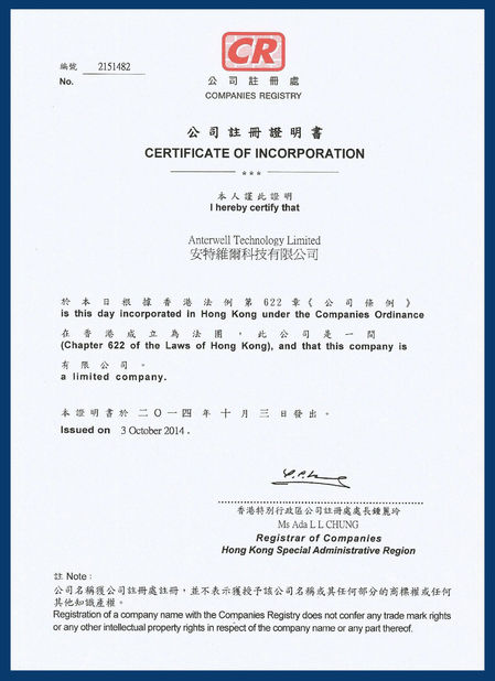
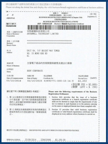
Anterwell Technology Ltd.
Anterwell Technology Ltd.
Large Original stock of IC Electronics Components, Transistors, Diodes etc.
High Quality, Reasonable Price, Fast Delivery.
Anterwell Technology Ltd.
Large Original stock of IC Electronics Components, Transistors, Diodes etc.
High Quality, Reasonable Price, Fast Delivery.
Product Details:
Payment & Shipping Terms:
|
| VIN Differential: | ±1.2V | Supply Voltage (V+ - V− ): | 13.2V |
|---|---|---|---|
| Voltage At Input Pins: | V+ +0.5V, V− −0.5V | Soldering Information: | 235˚C |
| Wave Soldering (10 Sec.): | 260˚C | ||
| High Light: | diode rectifier circuit,signal schottky diode |
||
![]() Features
Features
► Gain bandwidth (LMH6624) 1.5GHz
► Input voltage noise 0.92nV/
► Input offset voltage (limit over temp) 700uV
► Slew rate 350V/µs n Slew rate (AV = 10) 400V/µs
► HD2 @ f = 10MHz, RL = 100Ω −63dBc
► HD3 @ f = 10MHz, RL = 100Ω −80dBc
► Supply voltage range (dual supply) ±2.5V to ±6V
► Supply voltage range (single supply) +5V to +12V
► Improved replacement for the CLC425 (LMH6624)
► Stable for closed loop |AV| ≥ 10
General Description
The LMH6624/LMH6626 offer wide bandwidth (1.5GHz for single, 1.3GHz for dual) with very low input noise (0.92nV/ , 2.3pA/ ) and ultra low dc errors (100µV VOS, ±0.1µV/˚C drift) providing very precise operational amplifiers with wide dynamic range. This enables the user to achieve closed-loop gains of greater than 10, in both inverting and non-inverting configurations.
The LMH6624 (single) and LMH6626’s (dual) traditional voltage feedback topology provide the following benefits: balanced inputs, low offset voltage and offset current, very low offset drift, 81dB open loop gain, 95dB common mode rejection ratio, and 88dB power supply rejection ratio.
The LMH6624/LMH6626 operate from ± 2.5V to ± 6V in dual supply mode and from +5V to +12V in single supply configuration.
LMH6624 is offered in SOT23-5 and SOIC-8 packages. The LMH6626 is offered in SOIC-8 and MSOP-8 packages.
![]()
![]() INTRODUCTION
INTRODUCTION
The LMH6624/LMH6626 are very wide gain bandwidth, ultra low noise voltage feedback operational amplifiers. Their excellent performances enable applications such as medical diagnostic ultrasound, magnetic tape & disk storage and fiber-optics to achieve maximum high frequency signal-tonoise ratios. The set of characteristic plots in the "Typical Performance" section illustrates many of the performance trade offs. The following discussion will enable the proper selection of external components to achieve optimum system performance.
BIAS CURRENT CANCELLATION
To cancel the bias current errors of the non-inverting configuration, the parallel combination of the gain setting (Rg) and feedback (Rf ) resistors should equal the equivalent source resistance (Rseq) as defined in Figure 1. Combining this constraint with the non-inverting gain equation also seen in Figure 1, allows both Rf and Rg to be determined explicitly from the following equations: Rf = AVRseq and Rg = Rf /(AV-1)
When driven from a 0Ω source, such as the output of an op amp, the non-inverting input of the LMH6624/LMH6626 should be isolated with at least a 25Ω series resistor
As seen in Figure 2, bias current cancellation is accomplished for the inverting configuration by placing a resistor (Rb) on the non-inverting input equal in value to the resistance seen by the inverting input (Rf ||(Rg+Rs)). Rb should to be no less than 25Ω for optimum LMH6624/LMH6626 performance. A shunt capacitor can minimize the additional noise of Rb.
High Power Rectifier Diode 1N4756A , Silicon Planar Zener Diodes
Bridge Type Rectifier Diode 1N4007 50 to 1000 Volts 1.0 Ampere
1N4742A Silicon Planar Zener Diodes for Stabilized Power Supply
Power Programmable IC Chips XC6SLX100-3FGG484C Spartan-6 Family Overview
128K Bytes Sound IC Chip Programming ATMEGA128-16AU 8 Bit Microcontroller
EMC Programmable IC Chips Compliant Slew Rate Limited EI , Timer IC Chip
SMD Power Mosfet Module L7812CV TO-220 Power Trans Electronic Compoents
2SD1594 3 Pin Transistor NEC NPN Power Transistor Switching High Speed
2N5459 Power Mosfet Transistor N-Channel To-92 Original Stock FSC
