Anterwell Technology Ltd.
Anterwell Technology Ltd.
Large Original stock of IC Electronics Components, Transistors, Diodes etc.
High Quality, Reasonable Price, Fast Delivery.
Anterwell Technology Ltd.
Large Original stock of IC Electronics Components, Transistors, Diodes etc.
High Quality, Reasonable Price, Fast Delivery.
Product Details:
Payment & Shipping Terms:
|
| Internal Supply Voltage Relative To GND: | –0.5 To 1.32 V | Auxiliary Supply Voltage Relative To GND: | –0.5 To 3.00 V |
|---|---|---|---|
| Output Driver Supply Voltage Relative To GND: | –0.5 To 3.75 V | Input Reference Voltage Relative To GND: | –0.5 To VCCO + 0.5 V |
| Junction Temperature: | 125 °C | Soldering Temperature: | 220 °C |
| High Light: | programming ic chips,ic programmer circuit |
||
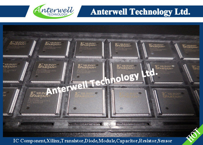
Spartan-3 FPGA Family
Introduction
The Spartan®-3 family of Field-Programmable Gate Arrays is specifically designed to meet the needs of high volume, cost-sensitive consumer electronic applications. The eight-member family offers densities ranging from 50,000 to five million system gates, as shown in Table 1.
The Spartan-3 family builds on the success of the earlier Spartan-IIE family by increasing the amount of logic resources, the capacity of internal RAM, the total number of I/Os, and the overall level of performance as well as by improving clock management functions. Numerous enhancements derive from the Virtex®-II platform technology. These Spartan-3 FPGA enhancements, combined with advanced process technology, deliver more functionality and bandwidth per dollar than was previously possible, setting new standards in the programmable logic industry.
Because of their exceptionally low cost, Spartan-3 FPGAs are ideally suited to a wide range of consumer electronics applications, including broadband access, home networking, display/projection and digital television equipment.
The Spartan-3 family is a superior alternative to mask programmed ASICs. FPGAs avoid the high initial cost, the lengthy development cycles, and the inherent inflexibility of conventional ASICs. Also, FPGA programmability permits design upgrades in the field with no hardware replacement necessary, an impossibility with ASICs.
The Spartan-3 FPGAs are the first platform among several within the Spartan-3 Generation FPGAs.
![]()
Features
• Low-cost, high-performance logic solution for high-volume, consumer-oriented applications
- Densities up to 74,880 logic cells
• SelectIO™ interface signaling
- Up to 633 I/O pins
- 622 Mb/s data transfer rate per I/O
- 18 single-ended signal standards
- 8 differential I/O standards including LVDS, RSDS
- Termination by Digitally Controlled Impedance
- Signal swing ranging from 1.14V to 3.465V
- Double Data Rate (DDR) support
- DDR, DDR2 SDRAM support up to 333 Mbps
• Logic resources
- Abundant logic cells with shift register capability
- Wide, fast multiplexers
- Fast look-ahead carry logic
- Dedicated 18 x 18 multipliers
- JTAG logic compatible with IEEE 1149.1/1532
• SelectRAM™ hierarchical memory
- Up to 1,872 Kbits of total block RAM
- Up to 520 Kbits of total distributed RAM
• Digital Clock Manager (up to four DCMs)
- Clock skew elimination
- Frequency synthesis
- High resolution phase shifting
• Eight global clock lines and abundant routing
• Fully supported by Xilinx ISE® and WebPACK™ software development systems
• MicroBlaze™ and PicoBlaze™ processor, PCI®, PCI Express® PIPE Endpoint, and other IP cores
• Pb-free packaging options
• Automotive Spartan-3 XA Family variant
Absolute Maximum Ratings
| Symbol | Description | Conditions | Min | Max | Units | |
|---|---|---|---|---|---|---|
| VCCINT | Internal supply voltage relative to GND | –0.5 | 1.32 | V | ||
| VCCAUX | Auxiliary supply voltage relative to GND | –0.5 | 3.00 | V | ||
| VCCO | Output driver supply voltage relative to GND | –0.5 | 3.75 | V | ||
| VREF | Input reference voltage relative to GND | –0.5 | VCCO + 0.5 | V | ||
| VIN | Voltage applied to all User I/O pins and Dual-Purpose pins relative to GND(2, 4) | Driver in a high-impedance state | Commercial | –0.95 | 4.4 | V |
| Industrial | –0.85 | 4.3 | V | |||
| Voltage applied to all Dedicated pins relative to GND(3) | All temp. ranges | –0.5 | VCCAUX + 0.5 | V | ||
| IIK | Input clamp current per I/O pin | –0.5 V < VIN < (VCCO + 0.5 V) | – | ±100 | mA | |
| VESD | Electrostatic Discharge Voltage pins relative to GND | Human body model | – | ±2000 | V | |
| Charged device model | – | ±500 | V | |||
| Machine model | – | ±200 | V | |||
| TJ | Junction temperature | – | 125 | °C | ||
| TSOL | Soldering temperature | – | 220 | °C | ||
| TSTG | Storage temperature | –65 | 150 | °C | ||
Notes:
1. Stresses beyond those listed under Absolute Maximum Ratings may cause permanent damage to the device. These are stress ratings only; functional operation of the device at these or any other conditions beyond those listed under the Recommended Operating Conditions is not implied. Exposure to Absolute Maximum Ratings conditions for extended periods of time adversely affects device reliability.
2. All User I/O and Dual-Purpose pins (DIN/D0, D1–D7, CS_B, RDWR_B, BUSY/DOUT, and INIT_B) draw power from the VCCO power rail of the associated bank. Keeping VIN within 500 mV of the associated VCCO rails or ground rail ensures that the internal diode junctions that exist between each of these pins and the VCCO and GND rails do not turn on. Table 31 specifies the VCCO range used to determine the max limit. Input voltages outside the -0.5V to VCCO+0.5V voltage range are permissible provided that the IIK input clamp diode rating is met and no more than 100 pins exceed the range simultaneously. The VIN limits apply to both the DC and AC components of signals. Simple application solutions are available that show how to handle overshoot/undershoot as well as achieve PCI compliance. Refer to the following application notes: "Powering and Configuring Spartan-3 Generation FPGAs in Compliant PCI Applications" (XAPP457) and "Virtex®-II Pro / Virtex-II Pro X 3.3V I/O Design Guidelines” (XAPP659).
3. All Dedicated pins (M0–M2, CCLK, PROG_B, DONE, HSWAP_EN, TCK, TDI, TDO, and TMS) draw power from the VCCAUX rail (2.5V). Meeting the VIN max limit ensures that the internal diode junctions that exist between each of these pins and the VCCAUX rail do not turn on. Table 31 specifies the VCCAUX range used to determine the max limit. When VCCAUX is at its maximum recommended operating level (2.625V), VIN max < 3.125V. As long as the VIN max specification is met, oxide stress is not possible. For information concerning the use of 3.3V signals, see the 3.3V-Tolerant Configuration Interface, page 46See XAPP459, “Eliminating I/O Coupling Effects when Interfacing Large-Swing Single-Ended Signals to User I/O Pins.”
4. For soldering guidelines, see "Device Packaging and Thermal Characteristics" (UG112) and "Implementation and Solder Reflow Guidelines for Pb-Free Packages" (XAPP427).
Stock Offer (Hot Sell)
| Part No. | Quantity | Brand | D/C | Package |
| P75NF75 | 11858 | ST | 14+ | TO-220 |
| P80C31SBAA | 3981 | PHILIPS | 00+ | PLCC44 |
| P80C31SBPN | 15810 | PHILIPS | 14+ | DIP-40 |
| P80C32UFAA | 3952 | PHILIPS | 04+ | PLCC44 |
| P87C51MB2BA/02 | 2102 | NXP | 11+ | PLCC44 |
| P89LPC925FDH | 2773 | NXP | 13+ | TSSOP-20 |
| P89LPC932A1FDH | 3177 | NXP | 15+ | TSSOP-28 |
| P89LPC936FDH | 8099 | NXP | 16+ | TSSOP-28 |
| PAL007E | 2744 | ST | 15+ | ZIP-25 |
| PALCE22V10H-15PC/4 | 9704 | AMD | 03+ | DIP-24 |
| PAM2320BECADJR | 11929 | AMD | 11+ | DIP-24 |
| PB5008 | 4281 | VISHAY | 10+ | DIP-4 |
| PBL3717A | 7258 | ST | 03+ | DIP-16 |
| PBSS5320T | 12000 | NXP | 05+ | SOT-23 |
| PC28F128P30TF65 | 4162 | MICRON | 10+ | BGA |
| PC357N1J000F | 84000 | SHARP | 16+ | SOP-4 |
| PC3H7CDJ000F | 29000 | SHARP | 15+ | SOP-4 |
| PC400 | 4586 | SHARP | 16+ | SOP-5 |
| PC452 | 86000 | SHARP | 14+ | SOP-4 |
| PC733H | 98000 | SHARP | 16+ | SOP-4 |
| PC817B | 15000 | SHARP | 16+ | DIP-4 |
| PC82573L | 2575 | INTEL | 15+ | BGA |
| PC901V | 7747 | SHARP | 16+ | DIP-6 |
| PC929 | 5320 | SHARP | 15+ | SOP-14 |
| PCA9306DCUR | 6604 | TI | 16+ | VSSOP-8 |
| PCA9515APWR | 17608 | TI | 10+ | TSSOP-8 |
| PCA9535CPW | 15881 | NXP | 07+ | TSSOP-24 |
| PCA9535D | 9775 | NXP | 06+ | SOP-24 |
| PCA9536D | 7718 | NXP | 06+ | SOP-8 |
| PCA9632TK | 7689 | NXP | 13+ | SOP-8 |
High Power Rectifier Diode 1N4756A , Silicon Planar Zener Diodes
Bridge Type Rectifier Diode 1N4007 50 to 1000 Volts 1.0 Ampere
1N4742A Silicon Planar Zener Diodes for Stabilized Power Supply
Power Programmable IC Chips XC6SLX100-3FGG484C Spartan-6 Family Overview
128K Bytes Sound IC Chip Programming ATMEGA128-16AU 8 Bit Microcontroller
EMC Programmable IC Chips Compliant Slew Rate Limited EI , Timer IC Chip
SMD Power Mosfet Module L7812CV TO-220 Power Trans Electronic Compoents
2SD1594 3 Pin Transistor NEC NPN Power Transistor Switching High Speed
2N5459 Power Mosfet Transistor N-Channel To-92 Original Stock FSC