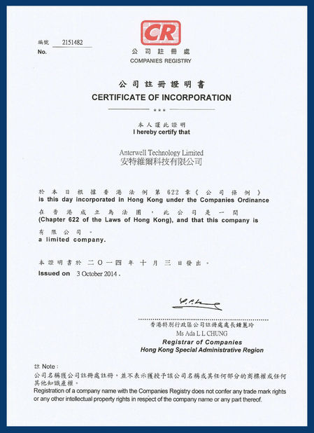
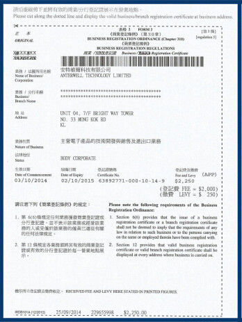
Anterwell Technology Ltd.
Anterwell Technology Ltd.
Large Original stock of IC Electronics Components, Transistors, Diodes etc.
High Quality, Reasonable Price, Fast Delivery.
Anterwell Technology Ltd.
Large Original stock of IC Electronics Components, Transistors, Diodes etc.
High Quality, Reasonable Price, Fast Delivery.
Product Details:
Payment & Shipping Terms:
|
| Supply Voltage: | −0.8 To +7.0 V | Supply Current: | 50 MA |
|---|---|---|---|
| Ground Supply Current: | 50 MA | Input Voltage: | −0.8 To VDD + 0.8 V |
| Input Current: | 10 MA | Total Power Dissipation: | 300 MW |
| High Light: | electronic integrated circuit,linear integrated circuits |
||
PCF8583 Clock and calendar with 240 x 8-bit RAM
General description
The PCF8583 is a clock and calendar chip, based on a 2048 bit static CMOS1 RAM organized as 256 words by 8 bits. Addresses and data are transferred serially via the two-line bidirectional I2C-bus. The built-in word address register is incremented automatically after each written or read data byte. Address pin A0 is used for programming the hardware address, allowing the connection of two devices to the bus without additional hardware.
The built-in 32.768 kHz oscillator circuit and the first 8 bytes of the RAM are used for the clock, calendar, and counter functions. The next 8 bytes can be programmed as alarm registers or used as free RAM space. The remaining 240 bytes are free RAM locations.
Features and benefits
Limiting values
In accordance with the Absolute Maximum Rating System (IEC 60134).
| Symbol | Parameter | Conditions | Min | Max | Unit | |
| VDD | supply voltage | −0.8 | +7.0 | V | ||
| IDD | supply current | - | 50 | mA | ||
| ISS | ground supply current | - | 50 | mA | ||
| VI | input voltage | −0.8 | VDD + 0.8 | V | ||
| II | input current | - | 10 | mA | ||
| IO | output current | - | 10 | mA | ||
| Ptot | total power dissipation | - | 300 | mW | ||
| Po | output power | - | 50 | mW | ||
| VESD | electrostatic discharge voltage | HBM | [1] | - | ±3000 | V |
| MM | [2] | - | ±200 | V | ||
| Ilu | latch-up current | [3] | - | 100 | mA | |
| Tstg | storage temperature | [4] | -65 | +150 | °C | |
| Tamb | ambient temperature | operating device | -40 | +85 | °C |
[1] Pass level; Human Body Model (HBM), according to Ref. 5 “JESD22-A114”.
[2] Pass level; Machine Model (MM), according to Ref. 6 “JESD22-A115”.
[3] Pass level; latch-up testing according to Ref. 7 “JESD78” at maximum ambient temperature (Tamb(max)).
[4] According to the NXP store and transport requirements (see Ref. 9 “NX3-00092”) the devices have to be stored at a temperature of +8 °C to +45 °C and a humidity of 25 % to 75 %. For long term storage products deviant conditions are described in that document.
Block diagram
![]()
Stock Offer (Hot Sell)
| Part No. | Quantity | Brand | D/C | Package |
| TL082ACDT | 17816 | ST | 16+ | SOP-8 |
| TL082CDT | 17366 | ST | 16+ | SOP-8 |
| TS271CDT | 16268 | ST | 13+ | SOP-8 |
| TS27L2IDT | 14548 | ST | 16+ | SOP-8 |
| TS912ID | 14504 | ST | 16+ | SOP-8 |
| TS912IDT | 17254 | ST | 09+ | SOP-8 |
| TS922IDT | 14482 | ST | 06+ | SOP-8 |
| TSM103AIDT | 10786 | ST | 15+ | SOP-8 |
| UC3525ADWTR | 5850 | ST | 10+ | SOP-8 |
| UC3842BD1R2G | 12992 | ST | 16+ | SOP-8 |
| NCP1337DR2G | 6652 | ON | 14+ | SOP-7 |
| TNY276GN | 16396 | POWER | 14+ | SOP-7 |
| TNY277GN-TL | 15668 | POWER | 15+ | SOP-7 |
| TNY286DG | 4004 | POWER | 13+ | SOP-7 |
| TNY287DG-TL | 16148 | POWER | 14+ | SOP-7 |
| TOP242GN | 17636 | POWER | 14+ | SOP-7 |
| TOP258GN | 9428 | POWER | 13+ | SOP-7 |
| TIL113SR2M | 13514 | FAIRCHILD | 16+ | SOP-6 |
| TGM-250NSRL | 18608 | HALO | 13+ | SOP-6 |
| TGM-240NSRL | 19024 | HALO | 14+ | SOP-6 |
| PVG612S | 28104 | IOR | 14+ | SOP-6 |
| PVT412ASP | 14916 | IR | 16+ | SOP-6 |
| T1-1T+ | 962 | MINI | 16+ | SOP-6 |
| TC2-72T+ | 2171 | MINI | 14+ | SOP-5 |
| PS8101-F3-AX | 18204 | RENESAS | 16+ | SOP-5 |
| PS9117A-F3-AX | 9552 | NEC | 09+ | SOP-5 |
| PS2732-1-F3 | 8808 | NEC | 16+ | SOP-4 |
| PS2811-1 | 11728 | RENENSAS | 16+ | SOP-4 |
| PS2501L-1-F3-A | 9500 | RENESAS | 13+ | SOP-4 |
| PS2701-1-F3-A | 12254 | RENESAS | 11+ | SOP-4 |
High Power Rectifier Diode 1N4756A , Silicon Planar Zener Diodes
Bridge Type Rectifier Diode 1N4007 50 to 1000 Volts 1.0 Ampere
1N4742A Silicon Planar Zener Diodes for Stabilized Power Supply
Power Programmable IC Chips XC6SLX100-3FGG484C Spartan-6 Family Overview
128K Bytes Sound IC Chip Programming ATMEGA128-16AU 8 Bit Microcontroller
EMC Programmable IC Chips Compliant Slew Rate Limited EI , Timer IC Chip
SMD Power Mosfet Module L7812CV TO-220 Power Trans Electronic Compoents
2SD1594 3 Pin Transistor NEC NPN Power Transistor Switching High Speed
2N5459 Power Mosfet Transistor N-Channel To-92 Original Stock FSC