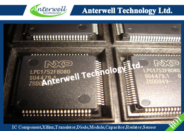
Microchips And Integrated Circuits LPC1752FBD80 32- bit ARM Cortex - M3 microcontroller
General description
The LPC1766 is an ARM Cortex-M3 based microcontroller for embedded applications featuring a high level of integration and low power consumption. The ARM Cortex-M3 is a next generation core that offers system enhancements such as enhanced debug features and a higher level of support block integration.
The LPC1766 operates at CPU frequencies of up to 80 MHz. The ARM Cortex-M3 CPU incorporates a 3-stage pipeline and uses a Harvard architecture with separate local instruction and data buses as well as a third bus for peripherals. The ARM Cortex-M3 CPU also includes an internal prefetch unit that supports speculative branching.
The peripheral complement of the LPC1766 includes 256 kB of flash memory, 64 kB of data memory, Ethernet MAC, USB Device/Host/OTG interface, 8-channel general purpose DMA controller, 4 UARTs, 2 CAN channels, 2 SSP controllers, SPI interface, 3 I 2C interfaces, 2-input plus 2-output I2S interface, 8 channel 12-bit ADC, 10-bit DAC, motor control PWM, Quadrature Encoder interface, 4 general purpose timers, 6-output general purpose PWM, ultra-low power RTC with separate battery supply, and up to 70 general purpose I/O pins.
The LPC1766 is pin-compatible to the LPC2366 ARM7-based microcontroller.
Features
- ARM Cortex-M3 processor, running at frequencies of up to 80 MHz. A Memory Protection Unit (MPU) supporting eight regions is included.
- ARM Cortex-M3 built-in Nested Vectored Interrupt Controller (NVIC).
- 256 kB on-chip flash programmimg memory. Enhanced flash memory accelerator enables high-speed 80 MHz operation with zero wait states.
- In-System Programming (ISP) and In-Application Programming (IAP) via on-chip boot loader software.
- 64 kB on-chip SRAM includes:
- 32 kB of SRAM on the CPU with local code/data bus for high-performance CPU access.
- Two 16 kB SRAM blocks with separate access paths for higher throughput. These SRAM blocks may be used for Ethernet, USB, and DMA memory, as well as for general purpose CPU instruction and data storage.
- Eight channel General Purpose DMA controller (GPDMA) on the AHB multilayer matrix that can be used with the SSP, I2S, UART, the Analog-to-Digital and Digital-to-Analog converter peripherals, timer match signals, and for memory-to-memory transfers.
- Multilayer AHB matrix interconnect provides a separate bus for each AHB master. AHB masters include the CPU, General Purpose DMA controller, Ethernet MAC, and the USB interface. This interconnect provides communication with no arbitration delays.
- Split APB bus allows high throughput with few stalls between the CPU and DMA.
- Serial interfaces:
- Ethernet MAC with RMII interface and dedicated DMA controller.
- USB 2.0 full-speed device/Host/OTG controller with dedicated DMA controller and on-chip PHY for device, Host, and OTG functions.
- Four UARTs with fractional baud rate generation, internal FIFO, DMA support, and RS-485 support. One UART has modem control I/O, and one UART has IrDA support.
- CAN 2.0B controller with two channels.
- SPI controller with synchronous, serial, full duplex communication and programmable data length.
- Two SSP controllers with FIFO and multi-protocol capabilities. The SSP interfaces can be used with the GPDMA controller.
- Two I2C-bus interfaces supporting fast mode with a data rate of 400 kbits/s with multiple address recognition and monitor mode.
- One I2C-bus interface supporting full I2C-bus specification and fast mode plus with a data rate of 1 Mbit/s with multiple address recognition and monitor mode.
- I 2S (Inter-IC Sound) interface for digital audio input or output, with fractional rate control. The I2S interface can be used with the GPDMA. The I2S interface supports 3-wire and 4-wire data transmit and receive as well as master clock input/output.
- Other peripherals:
- 70 General Purpose I/O (GPIO) pins with configurable pull-up/down resistors and a new, configurable open-drain operating mode.
- 12-bit Analog-to-Digital Converter (ADC) with input multiplexing among eight pins, conversion rates up to 1 MHz, and multiple result registers. The 12-bit ADC can be used with the GPDMA controller.
- 10-bit Digital-to-Analog Converter (DAC) with dedicated conversion timer and DMA support.
- Four general purpose timers/counters, with a total of eight capture inputs and ten compare outputs. Each timer block has an external count input and DMA support.
- One motor control PWM with support for three-phase motor control.
- Quadrature encoder interface that can monitor one external quadrature encoder.
- One standard PWM/timer block with external count input.
- Real-Time Clock (RTC) with a separate power domain and dedicated RTC oscillator. The RTC block includes 64 bytes of battery-powered backup registers.
- Watchdog Timer (WDT) resets the microcontroller within a reasonable amount of time if it enters an erroneous state.
- System tick timer, including an external clock input option.
- Repetitive interrupt timer provides programmable and repeating timed interrupts.
- Each peripheral has its own clock divider for further power savings.
- Standard JTAG test/debug interface for compatibility with existing tools. Serial Wire Debug and Serial Wire Trace Port options.
- Emulation trace module enables non-intrusive, high-speed real-time tracing of instruction execution.
- Integrated PMU (Power Management Unit) automatically adjusts internal regulators to minimize power consumption during Sleep, Deep sleep, Power-down, and Deep power-down modes.
- Four reduced power modes: Sleep, Deep-sleep, Power-down, and Deep power-down.
- Single 3.3 V power supply (2.4 V to 3.6 V).
- Four external interrupt inputs configurable as edge/level sensitive. All pins on PORT0 and PORT2 can be used as edge sensitive interrupt sources.
- Non-maskable Interrupt (NMI) input.
- Clock output function that can reflect the main oscillator clock, IRC clock, RTC clock, CPU clock, and the USB clock.
- The Wakeup Interrupt Controller (WIC) allows the CPU to automatically wake up from any priority interrupt that can occur while the clocks are stopped in deep sleep, power-down, and deep power-down modes.
- Processor wake-up from Power-down mode via interrupts from various peripherals.
- Brownout detect with separate threshold for interrupt and forced reset.
- Power-On Reset (POR).
- Crystal oscillator with an operating range of 1 MHz to 24 MHz.
- 4 MHz internal RC oscillator trimmed to 1 % accuracy that can optionally be used as a system clock.
- PLL allows CPU operation up to the maximum CPU rate without the need for a high-frequency crystal. May be run from the main oscillator, the internal RC oscillator, or the RTC oscillator.
- USB PLL for added flexibility.
- Code Read Protection (CRP) with different security levels.
- Available as 100-pin LQFP package (14 x 14 x 1.4 mm).
Applications
- eMetering
- Lighting
- Industrial networking
- Alarm systems
- White goods
- Motor control
Block diagram

Package outline
LQFP100: plastic low profile quad flat package; 100 leads; body 14 x 14 x 1.4 mm SOT407-1