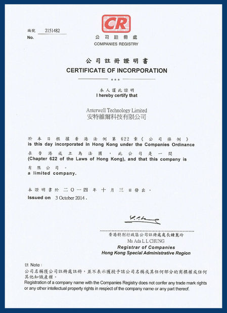
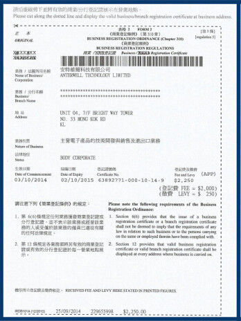
Anterwell Technology Ltd.
Anterwell Technology Ltd.
Large Original stock of IC Electronics Components, Transistors, Diodes etc.
High Quality, Reasonable Price, Fast Delivery.
Anterwell Technology Ltd.
Large Original stock of IC Electronics Components, Transistors, Diodes etc.
High Quality, Reasonable Price, Fast Delivery.
Product Details:
Payment & Shipping Terms:
|
| VDD To GND: | −0.3 V To +7 V | VDRIVE To GND: | −0.3 V To VDD + 0.3 V |
|---|---|---|---|
| Analog Input Voltage To GND: | −0.3 V To VDD + 0.3 V | Digital Input Voltage To GND: | −0.3 V To +7 V |
| Digital Output Voltage To GND: | −0.3 V To VDD + 0.3 V | REFIN To GND: | −0.3 V To VDD + 0.3 V |
| Input Current To Any Pin Except Supplies1: | ±10 MA | Storage Temperature Range: | −65°C To +150°C |
| High Light: | electronic chip board,electronic components ic |
||
16-Channel, 1 MSPS, 12-Bit ADC with Sequencer in 28-Lead TSSOP
FEATURES
Fast throughput rate: 1 MSPS
Specified for VDD of 2.7 V to 5.25 V
Low power at maximum throughput rates
5.4 mW maximum at 870 kSPS with 3 V supplies
12.5 mW maximum at 1 MSPS with 5 V supplies
16 (single-ended) inputs with sequencer
Wide input bandwidth
69.5 dB SNR at 50 kHz input frequency
Flexible power/serial clock speed management
No pipeline delays
High speed serial interface, SPI/QSPI™/MICROWIRE™/ DSP compatible
Full shutdown mode: 0.5 µA maximum
28-lead TSSOP and 32-lead LFCSP packages
FUNCTIONAL BLOCK DIAGRAM
![]()
GENERAL DESCRIPTION
The AD7490 is a 12-bit high speed, low power, 16-channel, successive approximation ADC. The part operates from a single 2.7 V to 5.25 V power supply and features throughput rates up to 1 MSPS. The part contains a low noise, wide bandwidth track-and-hold amplifier that can handle input frequencies in excess of 1 MHz.
The conversion process and data acquisition are controlled using CS and the serial clock signal, allowing the device to easily interface with microprocessors or DSPs. The input signal is sampled on the falling edge of CS, and conversion is also initiated at this point. There are no pipeline delays associated with the part.
The AD7490 uses advanced design techniques to achieve very low power dissipation at high throughput rates. For maximum throughput rates, the AD7490 consumes just 1.8 mA with 3 V supplies, and 2.5 mA with 5 V supplies.
By setting the relevant bits in the control register, the analog input range for the part can be selected to be a 0 V to REFIN input or a 0 V to 2 × REFIN input, with either straight binary or twos complement output coding. The AD7490 features 16 single-ended analog inputs with a channel sequencer to allow a preprogrammed selection of channels to be converted sequentially. The conversion time is determined by the SCLK frequency because this is also used as the master clock to control the conversion.
The AD7490 is available in a 32-lead LFCSP and a 28-lead TSSOP package.
PRODUCT HIGHLIGHTS
1. The AD7490 offers up to 1 MSPS throughput rates. At maximum throughput with 3 V supplies, the AD7490
dissipates just 5.4 mW of power.
2. A sequence of channels can be selected, through which the AD7490 cycles and converts.
3. The AD7490 operates from a single 2.7 V to 5.25 V supply. The VDRIVE function allows the serial interface
to connect directly to either 3 V or 5 V processor systems independent of VDD.
4. The conversion rate is determined by the serial clock, allowing the conversion time to be reduced through
the serial clock speed increase. The part also features various shutdown modes to maximize power efficiency
at lower throughput rates. Power consumption is 0.5 µA, maximum, when in full shutdown.
5. The part features a standard successive approximation ADC with accurate control of the sampling instant via
a CS input and once off conversion control.
ABSOLUTE MAXIMUM RATINGS TA = 25°C, unless otherwise noted.
| Parameter Rating |
|
VDD to GND −0.3 V to +7 V VDRIVE to GND −0.3 V to VDD + 0.3 V Analog Input Voltage to GND −0.3 V to VDD + 0.3 V Digital Input Voltage to GND −0.3 V to +7 V Digital Output Voltage to GND −0.3 V to VDD + 0.3 V REFIN to GND −0.3 V to VDD + 0.3 V Input Current to Any Pin Except Supplies1 ±10 mA Operating Temperature Ranges Commercial (B Version) −40°C to +85°C Storage Temperature Range −65°C to +150°C Junction Temperature 150°C LFCSP, TSSOP Package, Power Dissipation 450 mW θJA Thermal Impedance 108.2°C/W (LFCSP) 97.9°C/W (TSSOP) θJC Thermal Impedance 32.71°C/W (LFCSP) 14°C/W (TSSOP) Lead Temperature, Soldering Vapor Phase (60 sec) 215°C Infrared (15 sec) 220°C ESD 1 kV |
1 Transient currents of up to 100 mA do not cause SCR latch-up.
Stresses above those listed under Absolute Maximum Ratings may cause permanent damage to the device. This is a stress rating only; functional operation of the device at these or any other conditions above those indicated in the operational section of this specification is not implied. Exposure to absolute maximum rating conditions for extended periods may affect device reliability.
PIN CONFIGURATIONS AND FUNCTION DESCRIPTIONS
![]()
Pin Function Descriptions
|
Pin No. TSSOP LFCSP Mnemonic Description |
|
20 18 CS Chip Select. Active low logic input. This input provides the dual function of initiating conversions on the AD7490 and also frames the serial data transfer. 23 21 REFIN Reference Input for the AD7490. An external reference must be applied to this input. The voltage range for the external reference is 2.5 V ± 1% for specified performance. 22 20 VDD Power Supply Input. The VDD range for the AD7490 is from 2.7 V to 5.25 V. For the 0 V to 2 × REFIN range, VDD should be from 4.75 V to 5.25 V. 14, 21, 24 12, 19, 22 AGND Analog Ground. Ground reference point for all circuitry on the AD7490. All analog/digital input signals and any external reference signal should be referred to this AGND voltage. All AGND pins should be connected together. 13 to 5, 11 to 9, VIN0 to VIN15 Analog Input 0 through Analog Input 15. Sixteen single-ended 3 to 1, 7 to 2, analog input channels that are multiplexed into the on chip 28 to 25 31 to 26, track-and-hold. The analog input channel to be converted is 24 selected by using the address bits ADD3 through ADD0 of the control register. The address bits, in conjunction with the SEQ and SHADOW bits, allow the sequence register to be programmed. The input range for all input channels can extend from 0 V to REFIN or 0 V to 2 × REFIN as selected via the RANGE bit in the control register. Any unused input channels should be connected to AGND to avoid noise pickup. 19 17 DIN Data In. Logic input. Data to be written to the control register of the AD7490 is provided on this input and is clocked into the register on the falling edge of SCLK (see the Control Register section). 15 13 DOUT Data Out. Logic output. The conversion result from the AD7490 is provided on this output as a serial data stream. The bits are clocked out on the falling edge of the SCLK input. The data stream consists of four address bits indicating which channel the conversion result corresponds to, followed by the 12 bits of conversion data, which is provided by MSB first. The output coding can be selected as straight binary or twos complement via the CODING bit in the control register. 16 14 SCLK Serial Clock. Logic input. SCLK provides the serial clock for accessing data from the part. This clock input is also used as the clock source for the conversion process of the AD7490. 17 15 VDRIVE Logic Power Supply Input. The voltage supplied at this pin determines at what voltage the serial interface of the AD7490 operates. N/A EP EPAD Exposed Pad. Connect exposed pad to GND. |
High Power Rectifier Diode 1N4756A , Silicon Planar Zener Diodes
Bridge Type Rectifier Diode 1N4007 50 to 1000 Volts 1.0 Ampere
1N4742A Silicon Planar Zener Diodes for Stabilized Power Supply
Power Programmable IC Chips XC6SLX100-3FGG484C Spartan-6 Family Overview
128K Bytes Sound IC Chip Programming ATMEGA128-16AU 8 Bit Microcontroller
EMC Programmable IC Chips Compliant Slew Rate Limited EI , Timer IC Chip
SMD Power Mosfet Module L7812CV TO-220 Power Trans Electronic Compoents
2SD1594 3 Pin Transistor NEC NPN Power Transistor Switching High Speed
2N5459 Power Mosfet Transistor N-Channel To-92 Original Stock FSC
