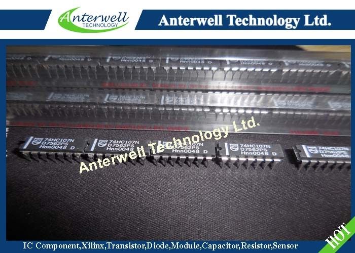
Anterwell Technology Ltd.
Anterwell Technology Ltd.
Large Original stock of IC Electronics Components, Transistors, Diodes etc.
High Quality, Reasonable Price, Fast Delivery.
Anterwell Technology Ltd.
Large Original stock of IC Electronics Components, Transistors, Diodes etc.
High Quality, Reasonable Price, Fast Delivery.
Product Details:
Payment & Shipping Terms:
|
| Output Capability: | Standard | Icc Category: | Flip-flop |
|---|---|---|---|
| QUICK REFERENCE DATA: | GND = 0 V; Tamb = 25 °C; Tr = Tf = 6 Ns | AC CHARACTERISTICS FOR 74HC: | GND = 0 V; Tr = Tf = 6 Ns; CL = 50 PF |
| AC CHARACTERISTICS FOR 74HCT: | GND = 0 V; Tf = Tf = 6 Ns; CL = 50 PF | PHILIPS: | NXP SEMICONDUCTORS |
| High Light: | electronics ic chip,integrated circuit components |
||
FEATURES
• Output capability: standard
• ICC category: flip-flop
GENERAL DESCRIPTION
The 74HC/HCT107 are high-speed Si-gate CMOS devices
and are pin compatible with low power Schottky TTL
(LSTTL). They are specified in compliance with JEDEC
standard no. 7A.
The 74HC/HCT107 are dual negative edge triggered
JK-type flip-flops featuring individual J, K, clock (nCP) and
reset (nR) inputs; also complementary Q and Q outputs.
The J and K inputs must be stable one set-up time prior to
the HIGH-to-LOW clock transition for predictable
operation.
The reset (nR) is an asynchronous active LOW input.
When LOW, it overrides the clock and data inputs, forcing
the Q output LOW and the Q output HIGH.
Schmitt-trigger action in the clock input makes the circuit
highly tolerant to slower clock rise and fall times.
QUICK REFERENCE DATA
GND = 0 V; Tamb = 25 °C; tr = tf = 6 ns
| SYMBOL | PARAMETER | CONDITIONS | TYPICAL | UNIT | |
| HC | HCT | ||||
| tPHL/ tPLH |
propagation delay nCP to nQ nCP to nQ nR to nQ, nQ |
CL = 15 pF; VCC = 5 V |
16 16 16 |
16 18 17 |
ns ns ns |
| fmax | maximum clock frequency | 78 | 73 | MHz | |
| CI | input capacitance | 3.5 | 3.5 | pF | |
| CPD | power dissipation capacitance per flip-flop | notes 1 and 2 | 30 | 30 | pF |
Notes
1. CPD is used to determine the dynamic power dissipation (PD in µW):
PD = CPD × VCC2 × fi + ∑ (CL × VCC2 × fo) where:
fi = input frequency in MHz
fo = output frequency in MHz
∑ (CL × VCC2 × fo) = sum of outputs
CL = output load capacitance in pF
VCC = supply voltage in V
2. For HC the condition is VI = GND to VCC
For HCT the condition is VI = GND to VCC − 1.5 V.
PIN DESCRIPTION
| PIN NO. | SYMBOL | NAME AND FUNCTION |
|
1, 8, 4, 11 2, 6 3, 5 7 12, 9 13, 10 14 |
1J, 2J, 1K, 2K 1Q, 2Q 1Q, 2Q GND 1CP, 2CP 1R, 2R VCC |
synchronous inputs; flip-flops 1 and 2 complement flip-flop outputs true flip-flop outputs ground (0 V) clock input (HIGH-to-LOW, edge-triggered) asynchronous reset inputs (active LOW) positive supply voltage |
![]()
![]()
High Power Rectifier Diode 1N4756A , Silicon Planar Zener Diodes
Bridge Type Rectifier Diode 1N4007 50 to 1000 Volts 1.0 Ampere
1N4742A Silicon Planar Zener Diodes for Stabilized Power Supply
Power Programmable IC Chips XC6SLX100-3FGG484C Spartan-6 Family Overview
128K Bytes Sound IC Chip Programming ATMEGA128-16AU 8 Bit Microcontroller
EMC Programmable IC Chips Compliant Slew Rate Limited EI , Timer IC Chip
SMD Power Mosfet Module L7812CV TO-220 Power Trans Electronic Compoents
2SD1594 3 Pin Transistor NEC NPN Power Transistor Switching High Speed
2N5459 Power Mosfet Transistor N-Channel To-92 Original Stock FSC