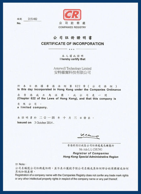
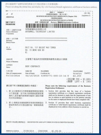
Anterwell Technology Ltd.
Anterwell Technology Ltd.
Large Original stock of IC Electronics Components, Transistors, Diodes etc.
High Quality, Reasonable Price, Fast Delivery.
Anterwell Technology Ltd.
Large Original stock of IC Electronics Components, Transistors, Diodes etc.
High Quality, Reasonable Price, Fast Delivery.
Product Details:
Payment & Shipping Terms:
|
| Internally Trimmed Offset Voltage: | 5 MV Max | Low Input Bias Current: | 50 PA |
|---|---|---|---|
| Wide Gain Bandwidth: | 4 MHz | N High Slew Rate: | 13 V/µs |
| Low Supply Current: | 7.2 MA | High Input Impedance: | 10^12Ω |
| High Light: | electronics ic chip,integrated circuit components |
||
LF147/LF347 Wide Bandwidth Quad JFET Input Operational Amplifiers
General Description
The LF147 is a low cost, high speed quad JFET input operational amplifier with an internally trimmed input offset voltage (BI-FET II™ technology). The device requires a low supply current and yet maintains a large gain bandwidth product and a fast slew rate. In addition, well matched high voltage JFET input devices provide very low input bias and offset currents.
The LF147 is pin compatible with the standard LM148. This feature allows designers to immediately upgrade the overall performance of existing LF148 and LM124 designs. The LF147 may be used in applications such as high speed integrators, fast D/A converters, sample-and-hold circuits and many other circuits requiring low input offset voltage, low input bias current, high input impedance, high slew rate and wide bandwidth. The device has low noise and offset voltage drift.
Features
Simplified Schematic Connection Diagram
![]()
DC Electrical Characteristics (Note 7)
| Symbol | Parameter | Conditions | LF147 | LF347B | LF347 | Units | ||||||
| Min | Typ | Max | Min | Typ | Max | Min | Typ | Max | ||||
| VOS | Input Offset Voltage |
RS=10 kΩ, TA=25˚C Over Temperature |
1
|
5 8 |
3
|
5 7 |
5
|
10 13 |
mV mV |
|||
| ∆VOS/∆T | Average TC of Input Offset Voltage | RS=10 kΩ | 10 | 10 | 10 | µV/˚C | ||||||
| IOS | Input Offset Current |
Tj =25˚C, (Notes 7, 8) Over Temperature |
25
|
100 25 |
25
|
100 4 |
25
|
100 4 |
pA nA |
|||
| IB | Input Bias Current |
Tj =25˚C, (Notes 7, 8) Over Temperature |
50
|
200 50 |
50
|
200 8 |
50
|
200 8 |
pA nA |
|||
| RIN | Input Resistance | Tj =25˚C | 1012 | 1012 | 1012 | Ω | ||||||
| AVOL | Large Signal Voltage Gain |
VS=±15V, TA=25˚C VO=±10V, RL=2 kΩ Over Temperature |
50
25 |
100
|
50
25 |
100
|
25
15 |
100
|
V/mV
V/mV |
|||
| VO | Output Voltage Swing | VS=±15V, RL=10 kΩ | ±12 | ±13.5 | ±12 | ±13.5 | ±12 | ±13.5 | V | |||
| VCM |
Input Common-Mode Voltage Range |
VS=±15V
|
±11
|
+15
-12 |
±11
|
+15
-12 |
±11
|
+15
-12 |
V
V |
|||
| CMRR | Common-Mode Rejection Ratio | RS≤10 kΩ | 80 | 100 | 80 | 100 | 70 | 100 | dB | |||
| PSRR | Supply Voltage Rejection Ratio | (Note 9) | 80 | 100 | 80 | 100 | 70 | 100 | dB | |||
| IS | Supply Current | 7.2 | 11 | 7.2 | 11 | 7.2 | 11 | mA | ||||
Note 2: Absolute Maximum Ratings indicate limits beyond which damage to the device may occur. Operating Ratings indicate conditions for which the device is functional, but do not guarantee specific performance limits.
Note 3: Unless otherwise specified the absolute maximum negative input voltage is equal to the negative power supply voltage.
Note 4: Any of the amplifier outputs can be shorted to ground indefinitely, however, more than one should not be simultaneously shorted as the maximum junction temperature will be exceeded.
Note 5: For operating at elevated temperature, these devices must be derated based on a thermal resistance of θjA.
Note 6: The LF147 is available in the military temperature range −55˚C≤TA≤125˚C, while the LF347B and the LF347 are available in the commercial temperature range 0˚C≤TA≤70˚C. Junction temperature can rise to Tj max = 150˚C.
Note 7: Unless otherwise specified the specifications apply over the full temperature range and for VS=±20V for the LF147 and for VS= ±15V for the LF347B/LF347. VOS, IB, and IOS are measured at VCM=0.
Note 8: The input bias currents are junction leakage currents which approximately double for every 10˚C increase in the junction temperature, Tj . Due to limited production test time, the input bias currents measured are correlated to junction temperature. In normal operation the junction temperature rises above the ambient temperature as a result of internal power dissipation, PD. Tj =TA+θjA PD where θjA is the thermal resistance from junction to ambient. Use of a heat sink is recommended if input bias current is to be kept to a minimum.
Note 9: Supply voltage rejection ratio is measured for both supply magnitudes increasing or decreasing simultaneously in accordance with common practice from VS = ± 5V to ±15V for the LF347 and LF347B and from VS = ±20V to ±5V for the LF147.
Note 10: Refer to RETS147X for LF147D and LF147J military specifications.
Note 11: Max. Power Dissipation is defined by the package characteristics. Operating the part near the Max. Power Dissipation may cause the part to operate outside guaranteed limits.
Note 12: Human body model, 1.5 kΩ in series with 100 pF
High Power Rectifier Diode 1N4756A , Silicon Planar Zener Diodes
Bridge Type Rectifier Diode 1N4007 50 to 1000 Volts 1.0 Ampere
1N4742A Silicon Planar Zener Diodes for Stabilized Power Supply
Power Programmable IC Chips XC6SLX100-3FGG484C Spartan-6 Family Overview
128K Bytes Sound IC Chip Programming ATMEGA128-16AU 8 Bit Microcontroller
EMC Programmable IC Chips Compliant Slew Rate Limited EI , Timer IC Chip
SMD Power Mosfet Module L7812CV TO-220 Power Trans Electronic Compoents
2SD1594 3 Pin Transistor NEC NPN Power Transistor Switching High Speed
2N5459 Power Mosfet Transistor N-Channel To-92 Original Stock FSC