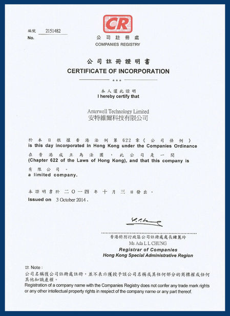
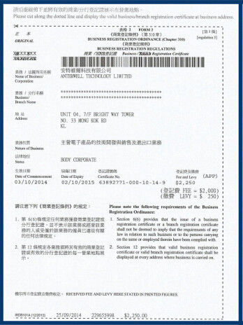
Anterwell Technology Ltd.
Anterwell Technology Ltd.
Large Original stock of IC Electronics Components, Transistors, Diodes etc.
High Quality, Reasonable Price, Fast Delivery.
Anterwell Technology Ltd.
Large Original stock of IC Electronics Components, Transistors, Diodes etc.
High Quality, Reasonable Price, Fast Delivery.
Product Details:
Payment & Shipping Terms:
|
| FEATURES: | Wide Operating Voltage Range Of 2 V To 6 V | FEATURES2: | Outputs Can Drive Up To 10 LSTTL Loads |
|---|---|---|---|
| FEATURES3: | Low Power Consumption, 40-µA Max ICC | Applications: | Typical Tpd = 15 Ns |
| Typical Applications 1: | ±4-mA Output Drive At 5 V | Package: | SOT23-5 |
| High Light: | electronics ic chip,integrated circuit ic |
||
Electronic Devices And Integrated Circuits 3V LVDS Single Amplifier IC Chip
General Description
The DS90LV011A is a single LVDS driver device optimized for high data rate and low power applications. The DS90LV011A is a current mode driver allowing power dissipation to remain low even at high frequency. In addition, the short circuit fault current is also minimized. The device is designed to support data rates in excess of 400Mbps (200MHz) utilizing Low Voltage Differential Signaling (LVDS) technology. The device is in both a 5-lead small outline transistor package and a new LLP-8 package with a 3mm x 3mm body size. The LVDS outputs have been arranged for easy PCB layout. The differential driver outputs provide low EMI with its typical low output swing of 350 mV. The DS90LV011A can be paired with its companion single line receiver, the DS90LV012A, or with any of National’s LVDS receivers, to provide a highspeed LVDS interface.
Features
n Conforms to TIA/EIA-644-A Standard n >400Mbps (200MHz) switching rates
n 700 ps (100 ps typical) maximum differential skew
n 1.5 ns maximum propagation delay
n Single 3.3V power supply
n ±350 mV differential signaling
n Power Off Protection (outputs in TRI-STATE)
n Pinout simplifies PCB layout
n Low power dissipation (23 mW @ 3.3V typical)
n SOT-23 5-lead package
n Leadless LLP-8 package (3x3 mm body size)
n SOT-23 version pin compatible with SN65LVDS1
n Fabricated with advanced CMOS process technology
n Industrial temperature operating range (−40˚C to +85˚C)
Connection Diagrams
![]() Absolute Maximum Ratings (Note 1)
Absolute Maximum Ratings (Note 1)
If Military/Aerospace specified devices are required, please contact the National Semiconductor Sales Office/ Distributors for availability and specifications.
Supply Voltage (VDD) −0.3V to +4V
LVCMOS input voltage (TTL IN) −0.3V to +3.6V
LVDS output voltage (OUT±) −0.3V to +3.9V
LVDS output short circuit current 24mA Maximum Package Power Dissipation @ +25˚C
LDA Package 2.26 W Derate LDA Package 18.1 mW/˚C above +25˚C Thermal resistance (θJA) 55.3˚C/Watt MF Package 902 mW Derate MF Package 7.22 mW/˚C above +25˚C Thermal resistance (θJA) 138.5˚C/Watt Storage Temperature −65˚C to +150˚C
Recommended Operating Conditions
| Min | Typ | Max | Units | |
| Supply Voltage (VDD) | 3.0 | 3.3 | 3.6 | V |
| Temperature (TA | −40 | +25 | +85 | ˚C |
Switching Characteristics (Continued)
Note 1: “Absolute Maximum Ratings” are those values beyond which the safety of the device cannot be guaranteed. They are not meant to imply that the devices should be operated at these limits. The table of “Electrical Characteristics” specifies conditions of device operation.
Note 2: Current into device pins is defined as positive. Current out of device pins is defined as negative. All voltages are referenced to ground except VOD.
Note 3: All typicals are given for: VDD = +3.3V and TA = +25˚C.
Note 4: Output short circuit current (IOS) is specified as magnitude only, minus sign indicates direction only.
Note 5: These parameters are guaranteed by design. The limits are based on statistical analysis of the device performance over PVT (process, voltage, temperature) ranges.
Note 6: CL includes probe and fixture capacitance.
Note 7: Generator waveform for all tests unless otherwise specified: f = 1 MHz, ZO = 50Ω, tr ≤ 1 ns, tf ≤ 1 ns (10%-90%).
Note 8: The DS90LV011A is a current mode device and only function with datasheet specification when a resistive load is applied to the drivers outputs.
Note 9: tSKD1, |tPHLD − tPLHD|, is the magnitude difference in differential propagation delay time between the positive going edge and the negative going edge of the same channel. Note 10: tSKD3, Differential Part to Part Skew, is defined as the difference between the minimum and maximum specified differential propagation delays. This specification applies to devices at the same VDD and within 5˚C of each other within the operating temperature range. Note 11: tSKD4, part to part skew, is the differential channel to channel skew of any event between devices. This specification applies to devices over recommended operating temperature and voltage ranges, and across process distribution. tSKD4 is defined as |Max − Min| differential propagation delay. Note 12: fMAX generator input conditions: tr = tf < 1 ns (0% to 100%), 50% duty cycle, 0V to 3V. Output criteria: duty cycle = 45%/55%, VOD > 250mV. The parameter is guaranteed by design. The limit is based on the statistical analysis of the device over the PVT range by the transitions times (tTLH and tTHL).
High Power Rectifier Diode 1N4756A , Silicon Planar Zener Diodes
Bridge Type Rectifier Diode 1N4007 50 to 1000 Volts 1.0 Ampere
1N4742A Silicon Planar Zener Diodes for Stabilized Power Supply
Power Programmable IC Chips XC6SLX100-3FGG484C Spartan-6 Family Overview
128K Bytes Sound IC Chip Programming ATMEGA128-16AU 8 Bit Microcontroller
EMC Programmable IC Chips Compliant Slew Rate Limited EI , Timer IC Chip
SMD Power Mosfet Module L7812CV TO-220 Power Trans Electronic Compoents
2SD1594 3 Pin Transistor NEC NPN Power Transistor Switching High Speed
2N5459 Power Mosfet Transistor N-Channel To-92 Original Stock FSC
