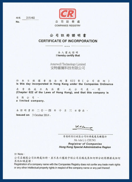
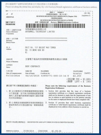
Anterwell Technology Ltd.
Anterwell Technology Ltd.
Large Original stock of IC Electronics Components, Transistors, Diodes etc.
High Quality, Reasonable Price, Fast Delivery.
Anterwell Technology Ltd.
Large Original stock of IC Electronics Components, Transistors, Diodes etc.
High Quality, Reasonable Price, Fast Delivery.
Product Details:
Payment & Shipping Terms:
|
| Working Temperature Range: | 40° C To + 125 °C | Series: | FM24CL64B-G |
|---|---|---|---|
| Package: | SOIC-8 | VDD POWER: | - 1 V To + 4.5 V |
| High Light: | integrated circuit ic,integrated circuit components |
||
FM24CL64B-GTR Automotive Temp. 64Kb Serial 3V F-RAM Memory
Features
64K bit Ferroelectric Nonvolatile RAM
Organized as 8192 x 8 bits
High Endurance 10 Trillion (1013 ) Read/Writes
NoDelay™ Writes
Advanced High-Reliability Ferroelectric Process
Fast Two-wire Serial Interface
Up to 1 MHz maximum bus frequency
Direct hardware replacement for EEPROM
Supports legacy timing for 100 kHz & 400 kHz
Low Power Consumption
Low Voltage Operation 3.0-3.6V
6 μA Standby Current (+85°C)
Industry Standard Configuration
Automotive Temperature -40C to +125C
Qualified to AEC Q100 Specification
8-pin “Green”/RoHS SOIC Package
Description
The FM24CL64B is a 64Kbit nonvolatile memory employing an advanced ferroelectric process. A ferroelectric random access memory or F-RAM is nonvolatile and performs reads and writes like a RAM. It provides reliable data retention for years while eliminating the complexities, overhead, and system level reliability problems caused by EEPROM and other nonvolatile memories. The FM24CL64B performs write operations at bus speed. No write delays are incurred. The next bus cycle may commence immediately without the need for data polling. In addition, the product offers write endurance orders of magnitude higher than EEPROM. Also, F-RAM exhibits much lower power during writes than EEPROM since write operations do not require an internally elevated power supply voltage for write circuits. These capabilities make the FM24CL64B ideal for nonvolatile memory applications requiring frequent or rapid writes. Examples range from data collection where the number of write cycles may be critical, to demanding industrial controls where the long write time of EEPROM can cause data loss. The combination of features allows more frequent data writing with less overhead for the system. The FM24CL64B provides substantial benefits to users of serial EEPROM, yet these benefits are available in a hardware drop-in replacement. The device is available in industry standard 8-pin SOIC package using a familiar two-wire (I2C) protocol. The device is guaranteed over the automotive temperature range of -40°C to +125°C.
Pin Configuration
![]()
![]()
Pin Description
| Pin Name | Type | Pin Description |
|---|---|---|
| A0-A2 | Input | Device Select Address 0-2: These pins are used to select one of up to 8 devices of the same type on the same two-wire bus. To select the device, the address value on the two pins must match the corresponding bits contained in the slave address. The address pins are pulled down internally |
| SDA | I/O | Serial Data/Address: This is a bi-directional pin for the two-wire interface. It is open-drain and is intended to be wire-OR‟d with other devices on the two-wire bus. The input buffer incorporates a Schmitt trigger for noise immunity and the output driver includes slope control for falling edges. An external pull-up resistor is required. |
| SCL | Input | Serial Clock: The serial clock pin for the two-wire interface. Data is clocked out of the part on the falling edge, and into the device on the rising edge. The SCL input also incorporates a Schmitt trigger input for noise immunity. |
| WP | Input | Write Protect: When tied to VDD, addresses in the entire memory map will be writeprotected. When WP is connected to ground, all addresses may be written. This pin is pulled down internally. |
| VDD | Supply | Supply Voltage |
| VSS | Supply | Ground |
Overview
The FM24CL64B is a serial F-RAM memory. The memory array is logically organized as a 8,192 x 8 bit memory array and is accessed using an industry standard two-wire interface. Functional operation of the F-RAM is similar to serial EEPROMs. The major difference between the FM24CL64B and a serial EEPROM with the same pinout relates to its superior write performance.
Memory Architecture
When accessing the FM24CL64B, the user addresses 8192 locations each with 8 data bits. These data bits are shifted serially. The 8192 addresses are accessed using the two-wire protocol, which includes a slave address (to distinguish other non-memory devices) and a 2-byte address. Only the lower 13 bits are used by the decoder for accessing the memory. The upper three address bits should be set to 0 for compatibility with higher density devices in the future. The access time for memory operation is essentially zero beyond the time needed for the serial protocol. That is, the memory is read or written at the speed of the two-wire bus. Unlike an EEPROM, it is not necessary to poll the device for a ready condition since writes occur at bus speed. That is, by the time a new bus transaction can be shifted into the part, a write operation will be complete. This is explained in more detail in the interface section below. Users expect several obvious system benefits from the FM24CL64B due to its fast write cycle and high endurance as compared with EEPROM. However there are less obvious benefits as well. For example in a high noise environment, the fast-write operation is less susceptible to corruption than an EEPROM since it is completed quickly. By contrast, an EEPROM requiring milliseconds to write is vulnerable to noise during much of the cycle. Note that it is the user‟s responsibility to ensure that VDD is within datasheet tolerances to prevent incorrect operation.
Two-wire Interface
The FM24CL64B employs a bi-directional two-wire bus protocol using few pins or board space. Figure 2 illustrates a typical system configuration using the FM24CL64B in a microcontroller-based system. The industry standard two-wire bus is familiar to many users but is described in this section. By convention, any device that is sending data onto the bus is the transmitter while the target device for this data is the receiver. The device that is controlling the bus is the master. The master is responsible for generating the clock signal for all operations. Any device on the bus that is being controlled is a slave. The FM24CL64B always is a slave device. The bus protocol is controlled by transition states in the SDA and SCL signals. There are four conditions including start, stop, data bit, or acknowledge. Figure 3 illustrates the signal conditions that specify the four states. Detailed timing diagrams are shown in the electrical specifications section.
![]()
High Power Rectifier Diode 1N4756A , Silicon Planar Zener Diodes
Bridge Type Rectifier Diode 1N4007 50 to 1000 Volts 1.0 Ampere
1N4742A Silicon Planar Zener Diodes for Stabilized Power Supply
Power Programmable IC Chips XC6SLX100-3FGG484C Spartan-6 Family Overview
128K Bytes Sound IC Chip Programming ATMEGA128-16AU 8 Bit Microcontroller
EMC Programmable IC Chips Compliant Slew Rate Limited EI , Timer IC Chip
SMD Power Mosfet Module L7812CV TO-220 Power Trans Electronic Compoents
2SD1594 3 Pin Transistor NEC NPN Power Transistor Switching High Speed
2N5459 Power Mosfet Transistor N-Channel To-92 Original Stock FSC